 COURSE PREVIEW
About this course
Are you preparing for a Design for Test (DFT) engineering role, studying for a VLSI/ASIC interview, or looking to strengthen your understanding of how modern chips are tested for manufacturing defects? This course is a focused, practice-based path to real DFT fluency.
Rather than another slow, video-based course, this is a hands-on practice test series built around 200+ carefully written multiple-choice questions, each with a detailed explanation for every answer option — not just the correct one. That means every question teaches you something, whether you get it right or wrong.
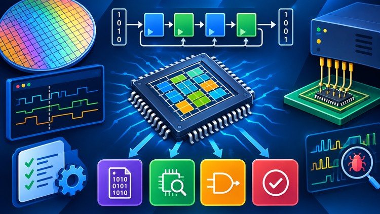
You'll work through six full practice exams that mix questions across all the core areas of Design for Test, including:
DFT fundamentals: fault models (stuck-at, transition, bridging), controllability, and observability
Scan design and scan chain architecture, insertion, and optimization
Automatic Test Pattern Generation (ATPG): sensitization, propagation, and compaction
Memory BIST (MBIST) and Logic BIST (LBIST), including March algorithms, LFSRs, and MISRs
Boundary scan (JTAG / IEEE 1149.1), including TAP controllers and board-level interconnect test
Test compression and test data volume reduction
Fault coverage, DPPM, and other test quality metrics
Advanced topics: IDDQ testing, at-speed delay test, core-based test (IEEE 1500), and ATE fundamentals
DFT power considerations, including shift power, capture power, and IR drop
This course is designed for VLSI/ASIC design engineers, DFT engineers, test engineers, and physical design engineers, as well as electrical engineering students and new graduates preparing for interviews in the semiconductor industry. Whether you're new to DFT or already working in the field and want to test and solidify what you know, these practice tests will help you build genuine command of the material through repetition, spaced review, and active recall.
No prior DFT experience is required — just a basic understanding of digital logic. By the end of this course, you'll be able to confidently discuss and apply scan design, ATPG concepts, BIST architectures, boundary scan, and test quality metrics used in real-world chip design and test engineering.
What you'll learn
- Master core DFT concepts: fault models, controllability/observability, scan design, and ATPG fundamentals used in real chip design flows
- Understand Memory BIST, Logic BIST, and boundary scan (JTAG/IEEE 1149.1) architectures used to test embedded memories, logic, and I/O
- Apply test compression, fault coverage, and DPPM/defect-level concepts to evaluate and optimize real-world test strategies
- Build confidence with at-speed testing, IDDQ, core-based test (IEEE 1500), and DFT power considerations through practice questions
Before you begin
- A basic understanding of digital logic (gates, flip-flops, and combinational/sequential circuits) is helpful but not required. No prior DFT or VLSI industry experience is needed — each question includes a detailed explanation for every answer option, so you'll build your understanding of Design for Test concepts as you go, regardless of your starting point.
Who this is for
- This course is designed for VLSI/ASIC design engineers, DFT engineers, test engineers, and physical design engineers looking to strengthen or validate their Design for Test knowledge. It's also well suited to electrical engineering students and new graduates preparing for interviews in the semiconductor industry, as well as anyone transitioning into a DFT-focused role who wants a structured, practice-based way to build confidence across scan design, ATPG, BIST, boundary scan, and test quality metrics. Whether you're brushing up before an interview or reinforcing concepts learned on the job, these practice tests are built to help you learn actively through repetition and detailed explanations rather than passive video-watching.
How do you feel about this course?
Share your reaction. Select one emoji to leave or update your rating.
Please wait 30 seconds to explore this course.
This course opens on an external website.
Join the conversation
Share a thought or question. No account required.
Be the first to share your thoughts.